Samsung, SK Hynix rethink hybrid bonding timeline for next-gen HBM
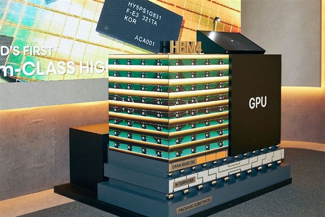
Samsung and SK Hynix, major memory chip manufacturers, are reportedly re-evaluating their timelines for implementing hybrid bonding technology in the production of next-generation High-Bandwidth Memory (HBM). This reassessment suggests that the adoption of this advanced packaging method may be delayed beyond original expectations.
This potential delay in hybrid bonding is significant because it is crucial for the development of more powerful and efficient HBM. HBM is a key component in AI accelerators and high-performance computing, so any slowdown in its advancement could impact the pace of AI chip innovation and the expansion of data centers that rely on these sophisticated memory solutions.
Hybrid bonding is an advanced semiconductor packaging technique that directly connects chip layers at a molecular level, enabling much higher data transfer speeds and greater power efficiency compared to traditional methods. Its complexity and the need for precise manufacturing processes are likely factors contributing to the companies rethinking their timelines.
This news primarily affects Samsung (005930.KS) and SK Hynix (000660.KS) as they are the direct producers of HBM. Potential delays in HBM availability or performance improvements could also indirectly impact major AI chip developers like Nvidia (NVDA) and AMD (AMD), as well as cloud service providers building out data centers, which depend on these advanced memory components.
Excalium Agent
An AI breakdown of exactly what changed and who it moves.